In the Parallel and Distributed System Architecture TRC Laboratory, we are developing the RHiNET network (RWCP High Performance Network) for achieving high-performance parallel processing by connecting personal computers and workstations.
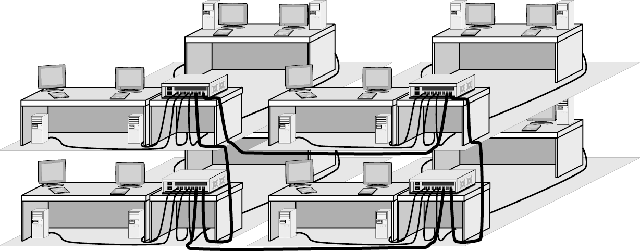
Consisting of a network interface mounted on the I/O bus of personal computers and workstations, a high-speed network switch and an optical interconnection between them, RHiNET realizes high-performance parallel processing by connecting personal computers and workstations on one or more floors of a building as shown in Figure 1.

The objective of RHiNET is not only to connect the computers installed in one location such as a cluster system, but also to connect computers distributed within a building or on a single floor, just like the conventional LAN system. For this, we need a link that is long enough for a free connection structure (topology) and LAN environment. In addition, to support high-performance computation it provides high bandwidth and low latency, as well as guarantees arrival order of packets. In addition, the network interface offers various communication functions that support parallel processing.
The development of RHiNET is divided into two stages: RHiNET-1 which uses a 1Gbps-class optical interconnection, and RHiNET-2 which uses an 8Gbps-class optical interconnection.
We have completed the development of the RHiNET-1 hardware and are currently evaluating the implementation of the communication protocol. In cooperation with the Optical Interconnection Hitachi Laboratory, we are developing a prototype ASIC switch for RHiNET-2 and conducting transmission tests.
RHiNET-1 uses a 1 to 1.3Gbps optical interconnection or the optical link used in Gigabit Ethernet. We developed the RHiNET-1/NI network interface and ASIC RHiNET-1/SW switch for RHiNET-1.

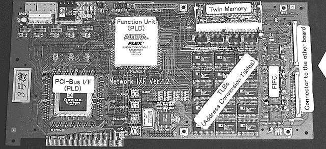
RHiNET-1/NI (Fig. 2) is a network interface which fits in a PCI bus and uses a PLD (Programmable Logic Device) as a controller. Implementing and evaluating various communications protocols are enabled by changing the settings of the PLD.
This interface contains address conversion tables (TLBs), and supports zero-copy communication with an arbitrary-size region. By being able to simultaneously access four memory banks, it can carry out operations such as address conversion as well as data transfer.
One of the memory banks is a large-capacity SDRAM. When temporarily copying the data held by other computers to the memory on a host, the original data are stored in this SDRAM. When writing back, by comparing the modified data on the SDRAM with the original data we can actually write back only the parts that have been modified. This realizes the implementation of a multiple writer using hardware.
RHiNET-1/SW (Fig. 3) is composed of a single-chip ASIC switch and can be connected to 8 sets of optical interconnection module or a Gigabit Ethernet transceiver. It has sufficient transfer bandwidth for a 32bit/33MHz PCI bus, which is the standard I/O bus of current PCs. By using a virtual channel cache method, deadlocks are prevented in a free connection structure and FIFO communication is achieved. It also has such characteristics as a multi-cast function, and allows hot swapping of links.
Using the memory of an external switch chip to secure the memory for the large-capacity packet buffer, RHiNET-1/SW uses the virtual channel cache method using a small-capacity memory inside the chip as the cache.
In view of the performance improvements in personal computers and workstations in the future and the required performance for associated networks, we can predict that networks in the future must be much faster than current networks.
In the application field of parallel processing, there are many problems that require faster speed when copying a large memory such as a matrix calculation. To improve the total performance of the whole system, we need a network that can copy to and from memory at the speed as close to the bandwidth of the memory as possible. The bandwidth of the memory of a conventional PC has reached 8.5Gbps (133MHz, 64bit) at maximum, and a network with a higher bandwidth, more than one memory bank and memory of RAMBUS method is about to appear.
On the other hand, the standard of the bandwidth of 10 Gbps-class such as for PCIX and System I/O, etc. are decided when planning the I/O part of a PC that contains the network interface. In the near future, regular personal computers and workstations in offices and laboratories will be equipped with network interfaces of several giga-bits.
In these circumstances, a network that surpasses the performance of RHiNET-1 will be required in the near future. We are therefore developing RHiNET-2 that is a higher-performance network using high-speed optical interconnection.
The RHiNET-2/NI network interface uses an ASIC as a controller. With a large-capacity memory and protocol processing processor inside the ASIC, the contents of protocol processing can be programmed. It can also be connected directly with a 8Gbps-class optical interconnection. We are now preparing the fundamental design.
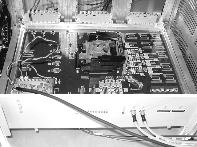
RHiNET-2/SW network switch has 8 input ports and 8 output ports that can be connected to an 8Gbps optical interconnection. Since it contains a large-capacity SRAM, external memory is not required. An LVDS (Low Voltage Differential Signaling) signal from 192 sets of 800Mbps connects between the optical interconnection module and the ASIC switch. Since a technology for wiring a high-speed signal line at a density as high as this on a substrate has not been created yet, technical development for this project is now being carried out at the Optical Interconnection Hitachi Laboratory. The first prototype (Fig. 4) of the ASIC switch has just been completed and transmission tests are being conducted. Since RHiNET-2/SW can connect high-speed optical interconnection of 8Gbps and optical interconnection of a 1Gbps-class simultaneously, it can connect to the RHiNET-1 network interface.
We will evaluate the performance of RHiNET-1 and based on the results, design RHiNET-2/NI. The RHiNET-2 system should become operational in FY 2000.
