Research on Network of Optoelectronic Processors Which Enables Arbitrary Parallel Signal Transimission among Processors
Shigeo Sugou
Optoelectronics Laboratory,NEC Corporation

To realize massively parallel computing, networks to link many processors and enable high-speed, large-capacity, and flexible data exchange are required, for which optical interconnection is expected to be a key technology. For instance, a massively parallel computer with the order of 1,000 processors may have more than 1,000 I/O pins on one processor board, and there are problems in implementation such as large cross-section of connectors and heavy cables, as well as the limits in bit rate and distance which cause another problem of frequency characteristics. To remedy these, optical connection's light-weight, high throughput, and long distance features will play a major role.
The Optoelectronics NEC Laboratory is working to create an optoelectronic processor network that combines the advantages of both electronics and optics, as an innovative high-performance optical interconnection, by studying optical interconnections to enable arbitrary optical parallel signal transmission among processors in a massively parallel computer.
Specifically, there are three research themes: development of the optical interface board for massively parallel computers, optoelectronic Smart Pixels as a key device, and three-dimensional optical connection elements to allow reconfigurable optical interconnections. The first theme is to develop an optical interconnection board for a massively parallel computer called RWC-1 under development by the RWCP Tsukuba Research Center with a goal of eliminating bottlenecks caused by pins which connect boards with optical interconnection technology. For the optoelectronic smart pixel theme, we are working on creating a long wavelength surface emitting laser as the key device that can be implemented in a large number of channels by two-dimensional integration and oscillates in the optical communication wavelength band. This will eliminate the bottlenecks among packages, rather than merely those among boards. It is a three-dimensional optical connection element that connects these functional elements integrated in two dimensions, and one of the goals of this research is to create a high-throughput transmission path with self-routing capability with which data can control its destination.
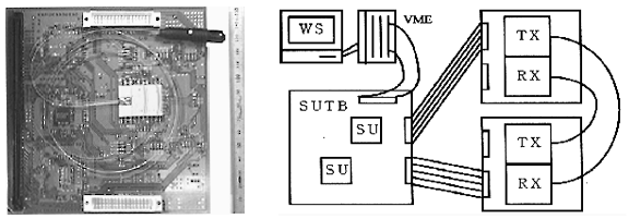
First, the recent research results of optical interface boards will be introduced. Fig. 1 (a) is a photo of a transmitter card of an optical data link subsystem mounted on the motherboard. It is 15 cm x 15 cm, and has LD array modules mounted at the center of the board which connect 6-pin tape fibers. It was fabricated as a basic component of the optical interface for RWC-1, and transmits a total of 4.8 Gbps (100Mb/s parallel 48 bits) of data signals on one optical tape fiber. In such parallel transmissions, data parallelism may be lost due to the skew in arrival timings of optical signals propagating in each fiber. Our card has a mechanism to compensate the skew of +/-15 ns (1.5T) so that parallel data can be treated as such after transmission with specifically-developed signal processing ICs.
Next, we conducted a data transmission experiment with this optical interface by using a testbed (SUTB:SU Test Bed) for data transmission experiment based on SU (Switching Unit), IC for data communication of RWC-1.

Fig. 1 (b) is a schematic diagram of the SUTB optical link experiment system. SUTB controls SU through the VMT Unit with WS instead of PE. We verified the packet transmission based on the RWC-1 protocol by transferring data from the Transmitter Card (TX) to the Receiver Card (RX) and comparing the contents of SU's data output register and input register after transmission. We also verified that the optical interface worked well without problems in that there were no errors during more than 17.5 hours with a connection distance of 10 m (equivalent to BER1x10-14 or less) by transmitting random packets generated continuously. Our experiments reached a transmission distance of up to 1 km with the same result.
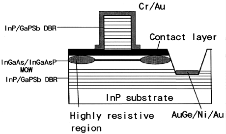
Next, our advanced research on the optoelectronic smart pixel/three-dimensional optical connection element will be introduced. The surface emitting LD, serving as a basic element of optoelectronic Smart Pixels, can be integrated in two dimensions, but has a problem in that it is difficult to attain good oscillation characteristics with the wavelength of 1.3 ɠm or 1.55 ɠm, suitable for optical communication. This was because the usual combination of optical semiconductors usable in this wavelength band could not yield a high delta in refractive index, and as a result it was difficult to fabricate a semiconductor multi-layered reflective mirror (DBR) with a reflective index of as high as 99% required for laser oscillation. To work around this problem, we proposed a new composition for a semiconductor which contains antimony (Sb), and worked on the development of a crystal growth technology to achieve a DBR with a reflexive index as high as 99%. Fig. 2 is a schematic diagram of the structure of this LD. A light emitting layer is put between DBRs composed of new material to form an optical resonator, and oscillating light emits in the direction of the substrate. Currently, we are working on the fabrication of a surface emitting LD with this DBR and the measurement of its characteristics.

We are also working on the design and fabrication of a selector which is responsible for routing by combining it with a light emitting array device based on this light emitting LD. The selector section is composed of GaAs-IC with its basic performance capable of 16ch addressable transmitter operations and each channel capable of 1Gb/s NRZ transmission. With this, optoelectronic crossbar switches can be implemented featuring low latency and high throughput. We are also studying transmission path and three-dimensional optical connection elements using spatial optics as a means of connecting Smart Pixels integrated in two dimensions. For this, we have developed the optoelectronic MCM (Multi-Chip Module) technology which enables alignment-free mounting of optics, and verified the basic operational principle of the 8ch-SDM switch by mounting two sets of 8 x 8 surface emitting laser (VCSEL) array optics in an alignment-free manner on an optoelectronic MCM substrate made of Al.
For the optical interface board, we will fabricate and test a RWC-1 processor board with optical interface. For the optoelectronic smart pixel/three-dimensional connection element, we will attempt to create a surface emitting LD which uses DBR in a new material and an optoelectronic smart pixel which uses this, and verify the scalability of switches and networks by continuing parallel transmission experiments with three-dimensional connection elements.