
Current Progress in Optical Interconnections

|
Shoichi HanataniDevelopment Center,Telecommunications Division, Hitachi, Ltd. |


|
Shoichi HanataniDevelopment Center,Telecommunications Division, Hitachi, Ltd. |
Optical fiber communication technology has been supporting our current information society since the technology became available as practical use in long-distance and large-capacity transmission systems in 1980ケs. It is now going to make an epoch toward the forthcoming 21st century. That is the progress as a new hardware technology which enables us to establish advanced information infrastructures capable of information processing faster than by several factors than the conventional technology.
The tremendous progress in information processing systems such as large computers and large capacity switches has been due to highly integrated and highly performed logic LSIs and highly dense surface-mount board technology. For further progress, however, the necessity of higher speed and higher density of wiring between or within these processing units is posing a new bottleneck. Also inside LSIs, there is a wiring bottleneck that increases the delay in signal transmission and the number of pins for input/output signals resulting in increased power consumption caused by higher integration and the ever-finer signal wiring. Optical interconnection technology is now drawing a wide attention as a most promising candidate to overcome these bottlenecks to implement high-speed and high-density wiring.
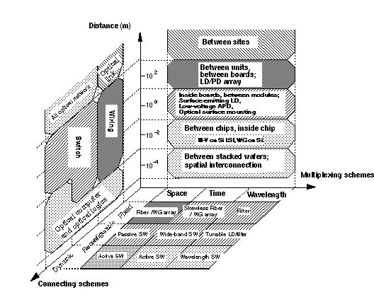
The optical interconnection involves a wide range of technologies as shown in Fig. 1. They may be classified into a number of technologies according to connecting distance, connection-switching schemes, and multiplexing schemes. The axis of connecting distance shows the areas to which the optical interconnection may be applied. The technology may be applied for connecting sites, units, boards, modules, and chips as well as within chips according to the layers of components of information processing units. There are three types of connection according to data transfer, speed and switching speed: (1) fixed connection, (2) circuit-switching or circuit rearrangement connection, and (3) dynamic connection for switching each bit. The optical interconnection system technology can be found on a plane formed by the axis along the connecting distances and connecting types. It ranges from optical wiring to all-optical network, cros s-point switch, optical computer and optical logic.
There are three multiplexing methods: space, time, and wavelength multiplexing. The key optical devices may be mapped to a plane formed by multiplexing methods and connecting types. Fiber array, optical switch, wavelength tunable light source and wavelength convertor are typical examples. Optical interconnection that meets the needs and maturity of these systems and device technologies will be put into practical use.
During the past several years, research and development has been aggressively conducted on optical wiring between units or boards using space-domain multiplexing (parallel transmission) fixed connection with the distance between 10 and 100 m. The conventional bundles of coaxial cables are being replaced by the bundles of optical fibers for high-speed, high-density signal wiring to implement high-performance, compact, and intelligent information processing systems.
This topic addresses the trend of research and development on the optical wiring between units and boards for parallel synchronous transmission using optical fiber arrays, and has a view of optical interconnection technologies.
Optical fiber not only enables low-loss wide-band transmission paths for high-speed and long-distance transmission, but it is suitable for high-speed, high-density wiring because of its lightweight, small diameter, resistant against immunity of EMI and grounding voltage intereference free. These feature are utilized for long-distance, high-capacity and high-density wiring for optical interconnection between units and boards.
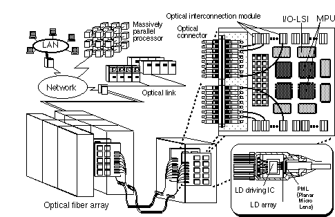
Fig. 2 is an image of a computer system using optical interconnection between units and boards. Instead of electrical connectors, optical connectors are used at the ends of boards for freely connecting units and boards with optical fiber arrays. A transmission and receiving optical modules that convert light data signals to electrical ones and vice versa are located near the logical I/O section. This makes the logical I/O section free from the design of high-speed, long-distance data transmission interface. For example, all logic circuits may be composed of CMOS technology instead of bipolar transistors that consume high power while providing a high driving performance. Thus, the optical interconnection not only resolves these wiring bottlenecks, but realizes high- performance logic circuits to further improve system performance or to implement high-performance systems never seen before.
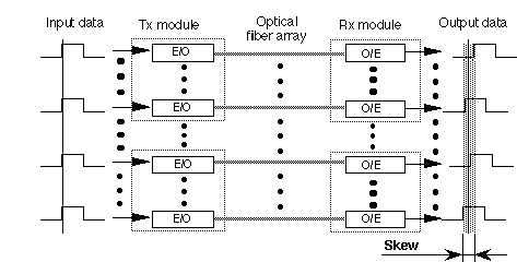
Fig. 3 shows the basic structure of an optical interconnection between units and boards. This is a synchronous parallel optical-fiber transmission system that regenerates data with the common clock using electricity-to-light and light-to-electricity conversion modules obtained by integrating multiple channels (e.g. 10 channels) in arrays and optical fiber arrays.
Technical challenges for implementing this technology are:
A number of approaches have been reported for these. As shown in Fig. 4, the types of modules may be classified into a pig-tail type, a receptacle type and an active connector type. All these types have advantages and disadvantages. The pig-tail type with pieces of fiber of 1 meter long is a main stream. Improving the throughput of boards requires the development of compact and low-loss optical connectors and adapters.
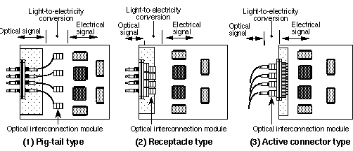
Table 1 shows the results of experiments reported so far on various combinations of light sources and fibers. They are LED (Light Emitting Diode) /MMF (Multi-Mode Fiber), LD (Laser-Diode) /MMF, SMF (Single-Mode Fiber) and VCSEL (Vertical Cavity Surface-Emitting Laser Diode)/MMF.
The research and development using LEDs is being performed actively because it is less dependent on temperature and is easy to optically couple with fiber. NEC reported transmission at 200 Mb/s/ch by developing an LED array capable of operation speed of up to 622 Mb/s with a low driving current of 25 mA. The mounting of an ATM (Asynchronous Transfer Mode) switch systems was attempted. AT&T has succeeded in transmitting at 200 Mb/s/ch with a 1-km distance by adjusting the length of each optical fiber in array. AT&T also developed 4:1 multiplexing and demultiplexing CMOS-LSI operating at 500 Mb/s/ch.
LD has optical power density larger than that of LED and is capable of high-speed operation, so it is promising for high-speed wiring at 200 Mb/s or higher. Variation of threshold current (Ith) among LDs and the variation in the light turn-on delay due to temperature changes make output waveform dependency on data patterns and skew issues. The development of an LD array with low threshold current and highly uniform characteristics is required to simplify a driving circuit as well as to reduce the dependency and the skew. It will also be effective to make LD driving (modulation plus bias) currents dependent on temperature. A high-speed transmission experiment using LDs was first reported by Toshiba. The skew of SMF was 2 ps/m or less and a fraction of MMF (15 ps/m). SMF is suitable for long distance (several 10 meters or longer) transmission.
Hitachi has reported an experiment on a high-speed long-distance transmission of 200 Mb/s/ch for 100 meters using LD/SMF. Hitachi also developed a low-skew LD array with Ith of 3mA or less, one tenth of the conventional ones. It also realized a small package measuring 0.76 cc by optical coupling method using a planar micro lens array. Experiments on high-speed transmission were reported by Fujitsu with 622 M, 1.2 Gb/s/ch, Hitachi with 800 Mb/s/ch and Siemens with 1 Gb/s or higher.
A large throughput was reported with the time-domain multiplexing method using the high-speed response characteristics of LD. This is a very promising method for a compact optical module with low power consumption and low price. Fujitsu reported the throughput of 3Gb/s by using a 6-channel integrated and 4:1 multiplexing method at 155 Mb/s/ch signals. The skew at high speed operation is logically handled by turning a frame bit into C bit and by arranging data accordingly. Clock supply and distribution methods, frame synchronization and the reduction of time required for the synchronization recovery will be technical issues to be developed in future.
VCSEL (surface light emitting LD) is being actively studied aorund the world, and the U.S.A. plays most active part in it. In VCSEL the adjustment of light emission patterns is easy to realize a highly efficient photo coupling with fiber. High performance and low cost will be possible because it facilitates on-wafer inspection and does not require cleaving process. GaAs compound materials used in VCSEL pose problems of high reliability and long life that need to be solved in future. OETC (GE, AT&T, Honeywell, IBM) and POLO (HP, Du Pont, AMP, USC, SDL) are doing research and development aided by ARPA (Advanced Research Project Agency). Their target is an optical link for WS with throughput of 10Gb/s or larger. Motorola has developed a transceiver-type receptacle optical module by developing a VCSEL by its own.
| NEC | AT&T | Toshiba | Siemens | NTT | Hitachi | Fujitsu | Motorola | OETC | POLO | |
|---|---|---|---|---|---|---|---|---|---|---|
| Year of Publication | '92.11 | '93.2 | '92 | '95.6 | '93.6 | '92.5 | '94.3 | '95.1 | `94 | `95.5 |
| Transmission speed(Mbit/s/ch) | 200 | 500 | 2000 | 1000 | 700 (2800) | 200 | 156 (625) | 150 | 500 | 1000 |
| Number of channels(ch/module) | 12 | 9 | 4 | 12 | 12 (4MUX) | 8 | 20 (4MUX) | 10 | 32 | 10 |
| Connection disance(m) | 100 | - | 26 | - | 250 | 100 | 400 | 30 | - | 300 |
| Skew(ns) | - | - | - | - | - | 2.0 | - | - | 1.5 | - |
| Power consumption | 580 | 1280 | 1080 | 110 | 1142 | 280 | 350 | 170typ. | 400 | 150 |
| Area(cm2/ch) | 6.16 | 5.56 | 7.19 | 0.09 | 6.2 | 0.31 | 2.98 | 0.59 | - | - |
| Light source | LED | LED | LD | LD | LD | LD | LD | VCSEL | VCSEL | VCSEL |
| Fiber | MMF | MMF | MMF | MMF | MMF | SMF | SMF | MMF | MMF | MMF |
| Wavelength (um) | 1.3 | 1.3 | 1.3 | 0.85 | 1.3 | 1.3 | 1.5 | 0.85 | 0.85 | 0.98 |
Although the optical interconnection using VCSEL has problems such as the reliability of the devices, skew and modal noise, it is promising for a compact and low price optical modules and the research and development efforts will be further intensified.
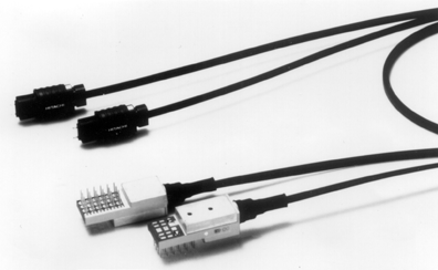
Photo 1 shows the external view of an optical interconnection module with 12 CMOS-Interface integrated channels and operating at +3.3V single power supply. The module comprises 11 data and clock channels and capable of transmitting with a distance of up to 100 m at 200 Mb/s/ch. It consumes a maximum of 200 mW per channel and operates at temperature range between 0 and 80 degrees C. It uses a push-on type (MPO) connector. It is applicable to various systems because it can transmit unformatted data. A switch board for ATM switching systems has been reported that uses 16 such modules with a throughput of 20 Gb/s. Researches are underway to use the module in a massively parallel computer RWC-1 that is being developed in this project (RWCP).
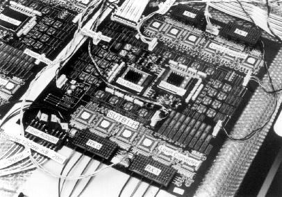
Photo 2 shows a testbed board for processor-node communication with 16 optical interconnector modules. It was confirmed that the board is capable of error-free transmission through a 20 m fiber and it is most likely to be applied to RWC-1. Currently, a processor board for optical interconnection is being developed.
While optical interconnectors are being put into practical use, we still have several issues. One issue is to reduce cost. The increase of quantity will be the biggest driving force to reduce cost of optical devices, packages and assembling. Therefore, the standardization of general-purpose optical interconnection should be pursued. Hardware (devices, surface mounting) and system designers must cooperate for this purpose. The next issue is reliability. A much higher reliability is required than those for the conventional optical communication to introduce this technology in a number of systems. Particularly the reliability of the laser, optical connectors and optical coupling are the key issue. Optical connectors tend to degrade after repeating connections and disconnections, so the development of a small, self-sealing and floating is to be pursued.
Optical interconnection using optical fibers for connecting units and boards allows a long-distance high-density wiring as well as releases load applied on output/input interfaces from LSI. It is certain that the technology will progress toward practical applications to realize high performance and multi function systems in near future. Then we will have a new technical issue of installing optical fibers. We will need optical backplane technology that introduces optical fibers and optical waveguides onto printed circuit boards and multi-chip module boards. A breakthrough is required for element technology such as surface light emitting laser, optical waveguide board and optical surface mounting. The development of these element technologies will start with optical interconnection technology between ICs and the inside ICs. Another key will be the integration of light source and photo-receiver devices.
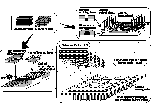
Fig. 5 is an image of 3-dimensional multi-chip optical interconnection module obtained by using these technologies. This will grow to become a key technology that supports the multi-media age in the 21st century.
The optical interconnection is a hardware technology to enable new information systems through integrating the semiconductor technology that has supported information society and the optical communication technology that will support the 21st century. RWCP will suggest an evolutional and the first in the world new information systems by further developing Japanケs optical interconnection technology. We hope the successful progress of RWCP and its results will contribute to the development of the Japanese information industry.