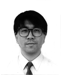
Jun Ohta
Optoelectronics MitsubishiLaboratory

|
Jun OhtaOptoelectronics MitsubishiLaboratory |
| Profile | |
| Affiliation: | Advanced Technology R&D Center, Mitsubishi Electric Corporation |
| Date of birth: | 15 June 1958 |
| Place of birth: | Gifu Prefecture |
| Background: | |
| 1981 | Graduated in Physical Engineering, Faculty of Engineering, University of Tokyo |
| 1983 | Completed Master of Science course at the Graduate School of Engineering, University of Tokyo. Joined Mitsubishi Electric Corp. |
| 1992-1993 | Guest Researcher at University of Colorado, USA. |
| Presently | researcher at the Advanced Technology R&D Center, Mitsubishi Electric Corp. |
I worked in the field of crystal growth of III-V-system compound semiconductors for optical devices during my Bachelor's and Master's degrees and for three years with Mitsubishi Electric Corp. After that, I became involved in research and development on optoelectronic integrated circuits (OEICs) and then in my current research on optical neural networks. Over the years, a single topic has remained central to my work, from crystal growth through devices to systems--and that is optoelectronics.
Light is a very attractive medium, and as is widely known, optical technology is now flourishing in fields such as optical communications and optical storage. Our topic is optical neural networks. We use optical technology capable of parallel processing and high speeds in the neural networks in the field of information processing.
However, it is not easy to exploit the potential that light has in this field. In fact, almost no practical systems have been developed in the field of optical computing. There are many possible reasons for this; one aspect is that there are no devices available that might be suitable for optical information processing, and another is the belated development of architecture suitable for optical technology.
To overcome these problems, we have so far been pursuing what device might be suitable for optical neural networks, and what sort of architecture is required. We had been working vigorously on research and development in optical neural devices for image processing using the two-dimensionality of light even several years before the start of the RWC project.
p This point was also an important topic during the period I spent as a guest researcher at the Optoelectronic Computing Systems Center (OCS) at University of Colorado for a year in 1992. While I was in the USA, the concepts of smart pixels and focal plane array processors (array devices fusing optical technology and electronic circuit technology) rapidly attracted attention. Various implementations, such as devices combining liquid crystals and silicon large-scale integration (Si-LSI), and devices integrating electronic circuits with optical devices on gallium arsenide (GaAs) emerged. The basic idea was, however, to take advantage of the strengths of both light (information transfer) and electrons (information processing). While I was there, I strongly agreed with the prevailing notion that not everything needs to be implemented using optical technology alone. Just before I returned to Japan, OCS experienced the considerable shake-up that was caused by this idea.
In our approach to optical neural devices for image processing using the two-dimensionality of light, the implementation is also achieved by combining optical technology and electronic technology. Our goal is to establish how to combine the promising medium of optical technology with mature electronic technology into technologies that are applicable to real world, and to extend them to construct a prototype, thus building practical systems.
I firmly believe that this RWC project will give rise to genuinely practical optical information processing systems.